English
 日本語
日本語 한국의
한국의 中文
中文PCBおよびPCBA設計、インテリジェント制御回路、そして生産最適化に10年以上携わってきました。世界中のエンジニアリングチームと緊密に連携し、信頼性、性能、そして製造性の向上に取り組んでいます。また、複雑なPCB技術をより理解しやすくするための実践的な知見を共有することにやりがいを感じています。

何を探していますか
?



Author
PCBおよびPCBA設計、インテリジェント制御回路、そして生産最適化に10年以上携わってきました。世界中のエンジニアリングチームと緊密に連携し、信頼性、性能、そして製造性の向上に取り組んでいます。また、複雑なPCB技術をより理解しやすくするための実践的な知見を共有することにやりがいを感じています。
Engaging professional pcb layout services early in the development cycle bridges the critical gap between theoretical hardware design and practical factory fabrication. In this article, we analyze the 7 most frequent DFM mistakes observed in high-density PCB layouts and provide actionable strategies to eliminate costly engineering change orders (ECOs) and avoid remanufacturing cycles.
1.Trace/Space vs. Copper Weight
The Risk: Specifying clearance on copper causes chemical over-etching or bridging.
DFM Solution: For copper, maintain ; for , keep . Consult our printed circuit board services for fine-pitch BGA tolerances.
2. Via-in-Pad Without Resin Fill
The Risk: Open vias in SMT pads cause solder wicking, leading to voids or open joints under BGAs.
DFM Solution: Specify IPC-4761 Type VII (Via Fill & Cap) in your circuit board design to ensure a flat, solderable pad surface.
3. Acid Traps (Acute Angles)
The Risk: Internal angles < 90 trap etching chemicals, causing long-term copper corrosion.
DFM Solution: Stick to 45 or curved traces and run automated DRC before Gerber export.
4. Solder Mask Slivers & Bleed
The Risk: Mask dams < 4 mil flake off and bridge pads; insufficient clearance covers solderable area.
DFM Solution: Enforce a minimum 3.5-4 mil solder mask damper. Professional pcb design services pre-configure these rules automatically.
5. Annular Ring Breakout
The Risk: Undersized pads lead to hole breakout during mechanical drilling, breaking circuit connectivity.
DFM Solution: Follow IPC-2221 Class 2 ( 2mil copper ring around the hole edge).
6. Solid Plane Connections (Tombstoning)
The Risk: Direct connection to copper planes without thermal relief drains heat unevenly, causing component tombstoning.
DFM Solution: Use 4-spoke thermal relief patterns on all plane connections for pcb custom jobs.
7. Missing Fiducials & Silk Overlap
The Risk: Missing optical marks lowers SMT accuracy; silkscreen on pads ruins solderability.
DFM Solution: Place global/local fiducials and set a 3 mil silkscreen-to-mask clearance.
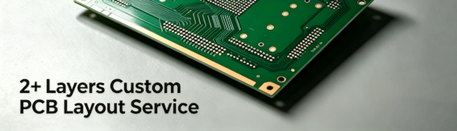
Need end-to-end circuit board design services, fast PCB prototyping, or turnkey PCBA? Ruichun conducts free automated DFM checks before manufacturing.
👉 Upload Gerber for a free quote: www.ruichunpcba.com
 IPv6 ネットワーク対応
伝言を残す
WhatsAppにスキャン :